




Two-dimensional semiconductor materials, represented by transition metal dichalcogenides (TMDCs), have the characteristics of extreme thickness, high mobility, and back-end heterogeneous integration. They are expected to continue Moore's law and realize integrated circuits with three-dimensional architecture. and industry attention. After nearly a decade of development, two-dimensional electronics has made great progress, but there are still challenges in the preparation of large-area single crystals, key device processes, and compatibility with mainstream semiconductor technologies.
Raziskovalna skupina profesorja Xinrana Wanga s Šole za elektronsko znanost in inženirstvo Univerze v Nanjingu se je osredotočila na zgornje probleme in raziskovala preboje v ključnih tehnologijah dvodimenzionalnih polprevodniških monokristalov in hetero- integracijo, ki je dala nove ideje za razvoj integriranih vezij v obdobju po-Moore. Ustrezni rezultati raziskav so bili nedavno objavljeni v Nature Nanotechnology.
Building "atomic terraces" down-to-earth, breaking through two-dimensional semiconductor single crystal epitaxy
Polprevodniški monokristalni materiali so temelj mikroelektronske industrije. V primerjavi z običajnimi 12-palčnimi monokristalnimi silicijevimi rezinami je priprava dvodimenzionalnih polprevodnikov-še vedno v majhnem-stopu in polikristalni fazi. Razvoj-visokokakovostnih-monokristalnih tankih filmov velike površine je prvi korak k dvodimenzionalnim-dimenzionalnim vezjem. . Vendar pa se med rastjo dvodimenzionalnih-materialov naključno generira na milijone mikroskopskih čipov in monolitni monokristalni material je mogoče dobiti le z nadzorom vseh čipov, da se ohrani strogo dosledna smer razporeditve.
Sapphire is a widely used substrate in the semiconductor industry and has outstanding advantages in mass production, low cost and process compatibility. The collaborating team proposed a scheme to artificially construct atomic-scale "terraces" by changing the direction of the atomic steps on the sapphire surface. The directional growth of TMDCs was achieved by the directional induced nucleation mechanism of "atomic terraces".
Based on this principle, the team achieved the epitaxial growth of a 2-inch MoS2 single crystal film for the first time in the world. Thanks to the improvement of material quality, the mobility of field effect transistors based on MoS2 single crystal is as high as 102.6 cm2/Vs, and the current density reaches 450 μA/μm, which is one of the highest comprehensive performances reported internationally. At the same time, the technology has good universality and is suitable for the preparation of single crystals of other materials such as MoSe2. This work has laid a material foundation for the application of TMDC in the field of integrated circuits.

Če gledamo navzgor proti zvezdam, dvodimenzionalni-polprevodniki prinašajo svetlobo v prihodnjo tehnologijo prikazovanja
Preboj enokristalnih materialov-površine-velike površine omogoča uporabo dvodimenzionalnih-polprevodnikov. V drugem delu, ki temelji na letih kopičenja polprevodniških raziskav tretje-generacije, v kombinaciji z najnovejšo dvodimenzionalno polprevodniško monokristalno rešitvijo, je zadružna ekipa Šole za elektroniko predlagala monolitno integrirano ultra -visoka-zaslon Micro LED z visoko ločljivostjo, ki temelji na gonilnem vezju tankoslojnega tranzistorja MoS2. Tehnične rešitve.
Micro LED se nanaša na tehnologijo, ki uporablja mikronske-LED-diode kot svetlobne{1}}oddajajoče slikovne enote in jih sestavlja s pogonskimi moduli, da tvori niz-zaslonov z visoko gostoto. V primerjavi s trenutnimi običajnimi zaslonskimi tehnologijami, kot sta LCD in OLED, ima Micro LED -generacijske prednosti v smislu svetlosti, ločljivosti, porabe energije, življenjske dobe, hitrosti odziva in toplotne stabilnosti ter je mednarodno priznana naslednja{ {4}}generacija zaslonske tehnologije.
Vendar pa se industrializacija Micro LED še vedno sooča s številnimi izzivi. Prvič, težko je izpolniti zahteve za vožnjo zaslonskih enot z{0}}veliko gostoto majhnih velikosti. Drugič, tehnologija množičnega prenosa, ki je priljubljena v industriji, težko zadosti razvojnim potrebam zaslonov z visoko{1}}ločljivostjo glede na stroške in donos. Zlasti pri aplikacijah z ultra-visoko- ločljivostjo, kot je AR/VR, ni potrebna le ločljivost, ki presega 3000 PPI, ampak morajo imeti tudi slikovne pike hitrejšo odzivno frekvenco.
The cooperative team aimed at the field of high-resolution micro-display, and proposed a technical solution for the 3D monolithic integration of MoS2 thin-film transistor driver circuit and GaN-based Micro LED display chip. The team developed a non-"massive transfer" low-temperature monolithic heterogeneous integration technology, using a nearly non-destructive large-size two-dimensional semiconductor TFT manufacturing process, to achieve a high-brightness, high-resolution microdisplay of 1270 PPI, which can meet the needs of future microdisplays. Display, vehicle display, visible light communication and other cross-field applications.
Among them, compared with the traditional two-dimensional semiconductor device process, the new process developed by the team improves the performance of thin film transistors by more than 200 percent , reduces the difference by 67 percent , and the maximum driving current exceeds 200 μA/μm, which is better than IGZO, LTPS and other commercial materials. It shows the huge application potential of two-dimensional semiconductor materials in the display driving industry. This work is the first in the world to integrate two emerging technologies of high-performance two-dimensional semiconductor TFT and Micro LED, which provides a new technical route for the future development of Micro LED display technology.
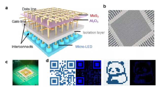
The above works are respectively named "Epitaxial growth of wafer-scale molybdenum disulfide semiconductor single crystals on sapphire" (corresponding authors are Prof. Wang Xinran and Prof. Wang Jinlan of Southeast University) and "Three dimensional monolithic Micro LED display driven by atomically-thin transistor matrix" (corresponding authors). It was published online in Nature Nanotechnology recently.
This series of work has been supported by projects such as Jiangsu Province's Frontier Leading Technology Basic Research Project, the National Natural Science Foundation of China, and the National Key RD Program. Changchun Institute of Optics and Mechanics, Chinese Academy of Sciences, Tianma Microelectronics Co., Ltd., Nanjing Huanxuan Semiconductor Co., Ltd., etc.


